LegacyVolta • 2017
V100
First GPU with Tensor Cores. Legacy architecture — mostly replaced by A100/H100 but still in use.
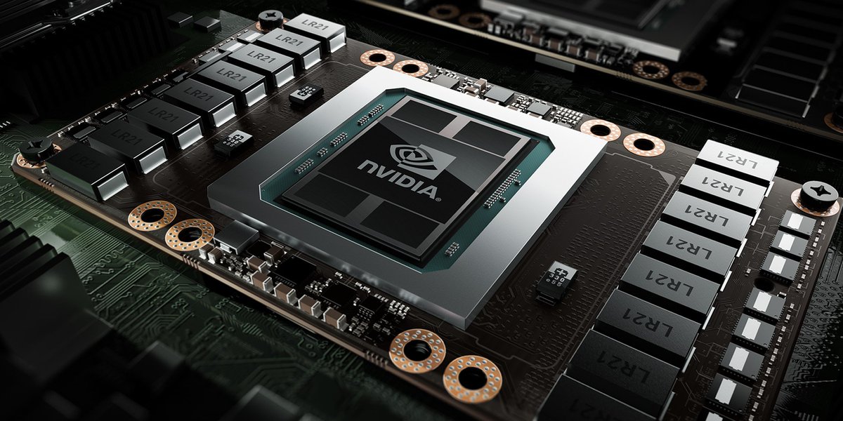
Technical Specifications
Architecture | Volta |
Release Year | 2017 |
Process Node | TSMC 12N |
Form Factor | SXM2 / PCIe Gen3 |
VRAM | 16 GB HBM2 / 32 GB HBM2 |
Memory Bandwidth | 900 GB/s |
Interconnect | NVLink 2 (300 GB/s) |
FP16 Performance | 125 TFLOPS (with Tensor Cores) |
FP32 Performance | 15.7 TFLOPS |
FP64 Performance | 7.8 TFLOPS |
TDP | 300W (SXM), 250W (PCIe) |
CUDA Cores | 5,120 |
Tensor Cores | 640 |
Transistors | 21.1 billion |
Die Size | 815 mm² |
Best Use Cases
- Legacy AI workloads
- HPC (legacy)
- Budget training
Quick Facts
FamilyVolta
ArchitectureVolta
Released2017
ProcessTSMC 12N
Form FactorSXM2 / PCIe Gen3
V100 — Frequently Asked Questions
What is the V100 GPU used for?
The V100 is best suited for: Legacy AI workloads, HPC (legacy), Budget training.
How much VRAM does the V100 have?
The V100 has 16 GB HBM2 / 32 GB HBM2 of VRAM.
What is the memory bandwidth of the V100?
The V100 has a memory bandwidth of 900 GB/s.
What interconnect does the V100 use?
The V100 uses NVLink 2 (300 GB/s).
When was the V100 released?
The V100 was released in 2017.