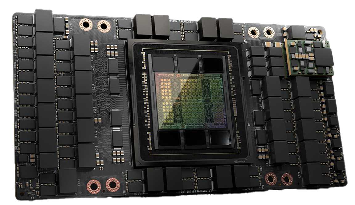
Industry standard (2022-2024)
NVIDIA
Hopper
NVIDIA Hopper is the industry standard for AI training, featuring HBM3 memory, the Transformer Engine for LLM workloads, and NVLink 4 interconnects (900 GB/s). The H100 is the most widely-deployed AI GPU in cloud computing today.
GPU Models in this Family
Click any card to expand detailed specifications
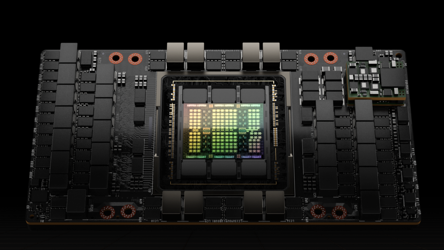
GH100
80 GB HBM33.35 TB/sSXM5 / PCIe Gen5
GH100
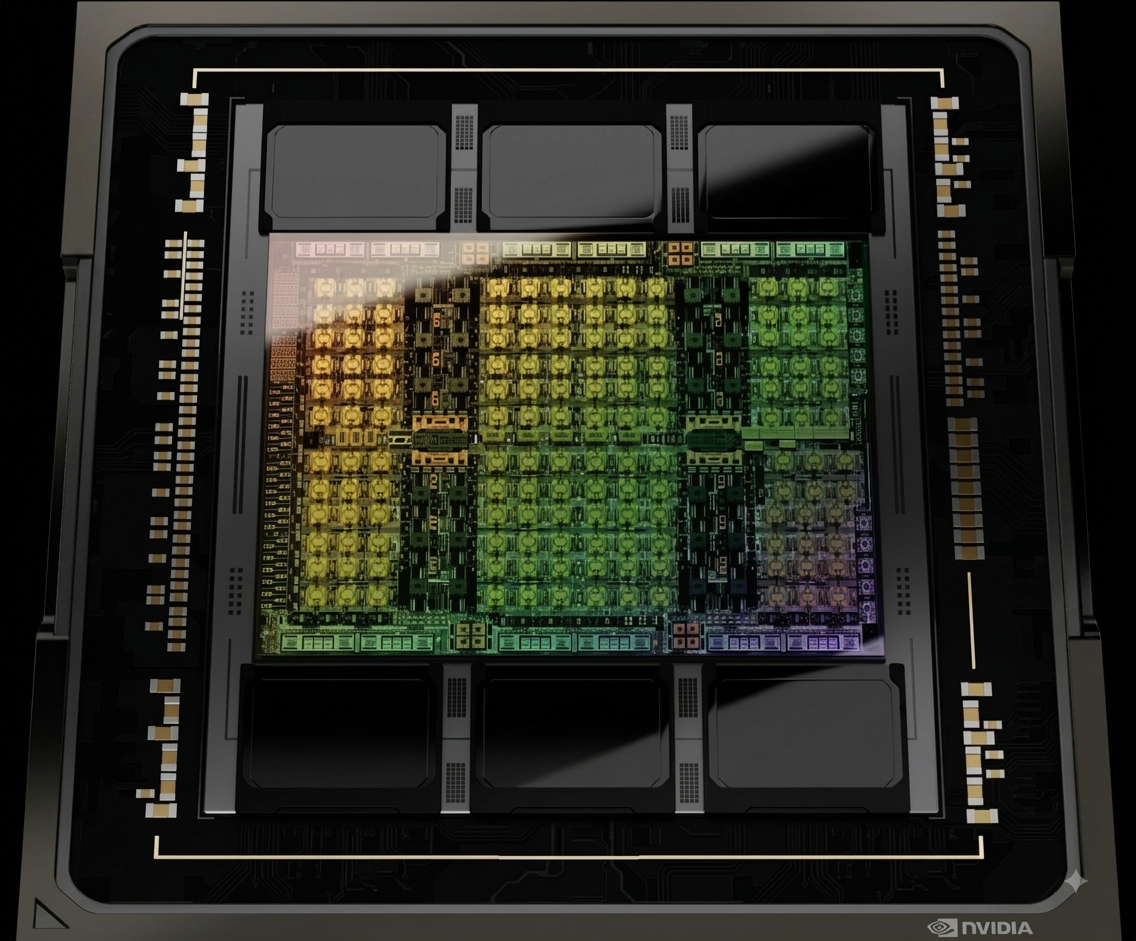
The GH100 is NVIDIA's Hopper architecture GPU silicon — the foundational chip that powers all H100 variants (SXM5, PCIe, NVL). Built on TSMC's custom 4N process with 80 billion transistors across an 814 mm² die, it introduced the Transformer Engine for accelerated LLM training and inference. The GH100 die is the largest and most complex GPU NVIDIA had shipped at its 2022 launch.
Transformer Engine, 4th-gen Tensor Cores, FP8 support, HBM3, DPX, NVLink 4
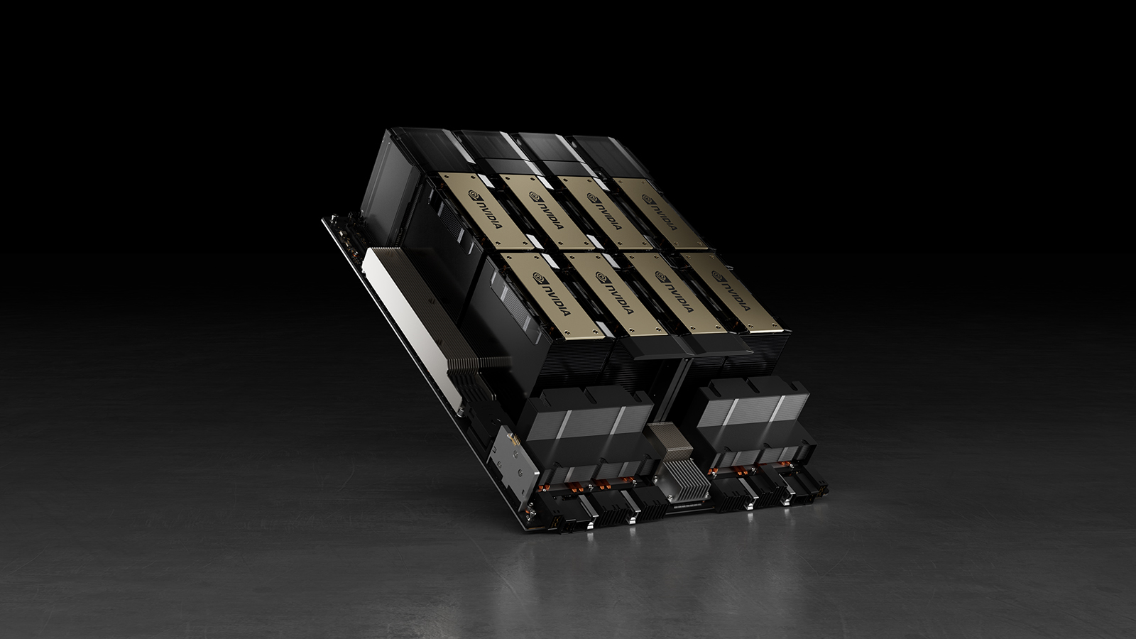
H100 SXM
80 GB HBM33.35 TB/sSXM5
H100 SXM
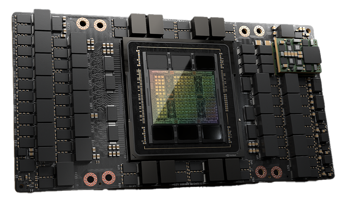
SXM5 form factor of H100. 80GB HBM3 with full NVLink 4 (900 GB/s). 700W TDP — the highest performance H100 variant for multi-GPU training.
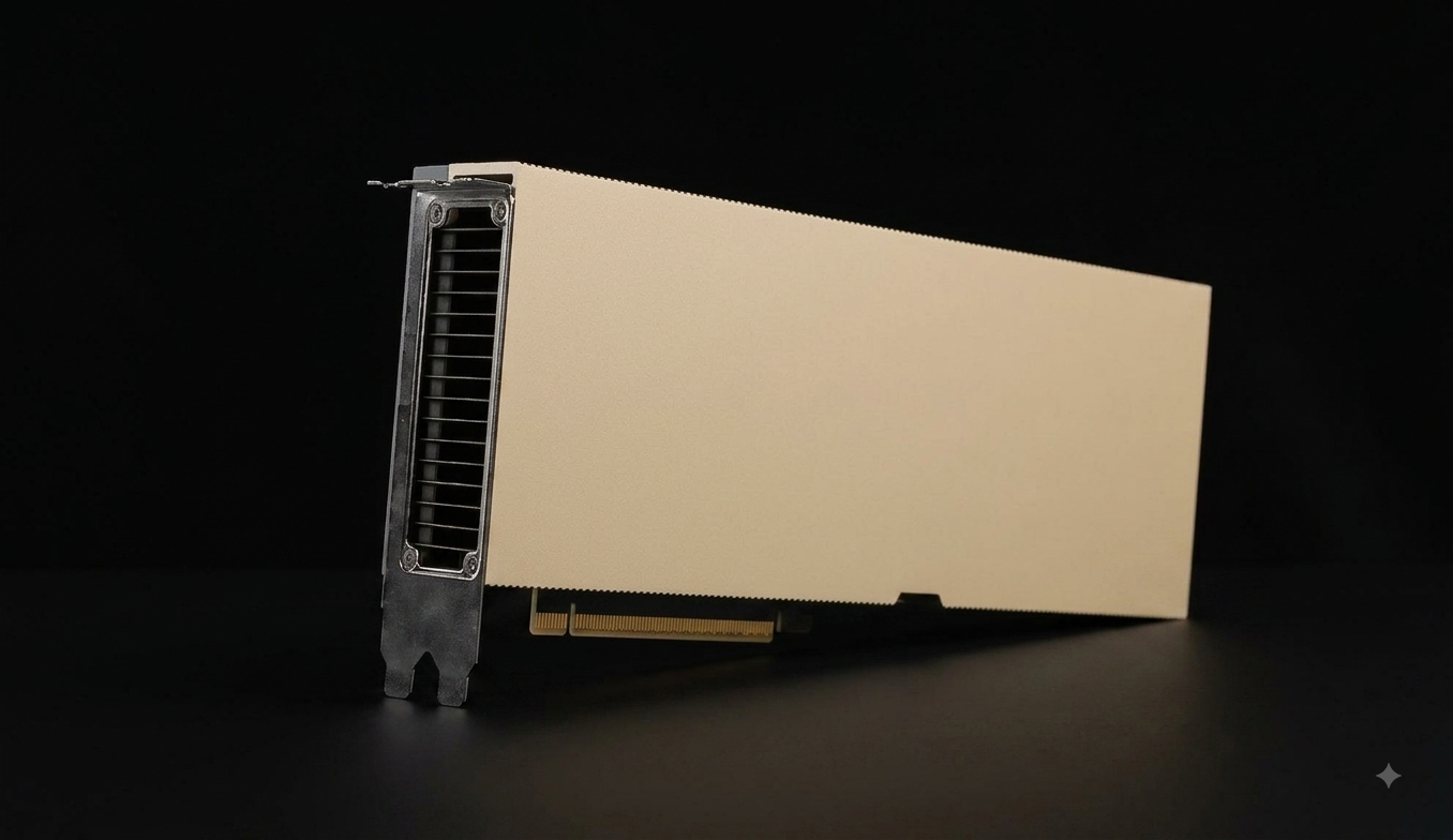
H100 PCIe
80 GB HBM33.35 TB/sPCIe Gen5
H100 PCIe
Standard PCIe Gen5 form factor of H100 (no NVLink). 350W TDP — lower performance than SXM but easier to deploy. No multi-GPU NVLink interconnect.
H100 NVL
94 GB HBM33.9 TB/sPCIe Gen5 (dual-slot)
H100 NVL
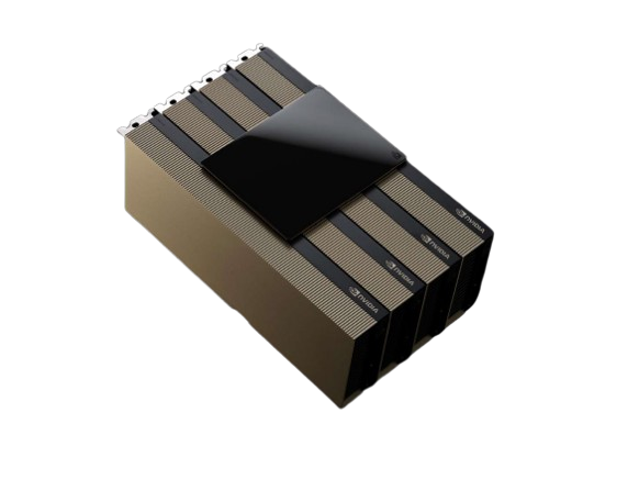
PCIe variant of H100 with 94GB HBM3 (more VRAM than SXM version). Uses NVLink bridge for multi-GPU on PCIe.
H200 SXM
141 GB HBM3e4.8 TB/sSXM5
H200 SXM
SXM5 form factor of H200. 141GB HBM3e with full NVLink 4 (900 GB/s). Highest bandwidth Hopper variant for large model training.
H200 NVL
141 GB HBM3e4.8 TB/sPCIe Gen5 (NVL)
H200 NVL
NVL Gen5 form factor of H200. 141GB HBM3e but no NVLink — uses NVL Gen5 (128 GB/s) instead. Lower power (350W) for environments without SXM.
GH200
144 GB HBM3e (or 96 GB HBM3)4.8 TB/s (HBM3e)Superchip (Grace CPU + Hopper GPU)
GH200
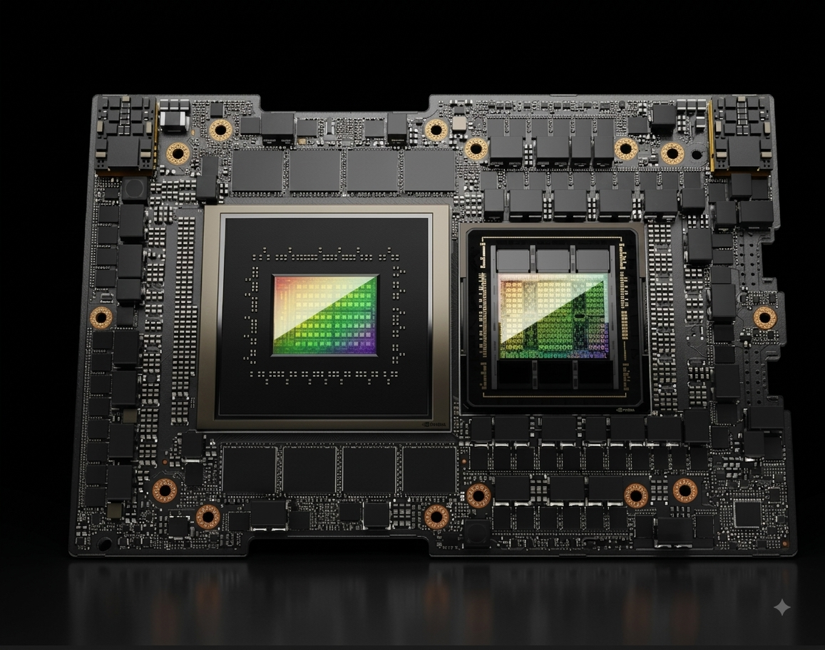
Grace + Hopper superchip with unified memory. Designed for giant-scale AI and HPC workloads.
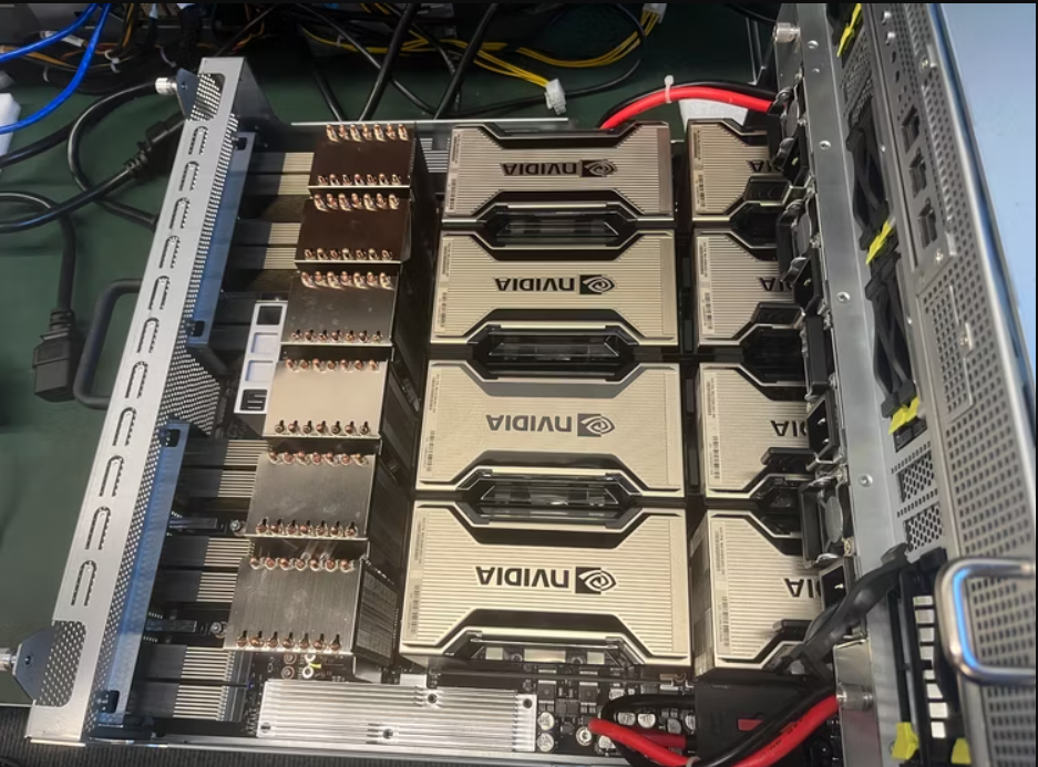
H800 SXM
80 GB HBM33.35 TB/sSXM5
H800 SXM
China export variant of the H100 SXM. Meets US export controls with reduced NVLink bandwidth (400 GB/s vs 900 GB/s) while retaining 80GB HBM3 and full compute density. Built for AI training in compliant regions.
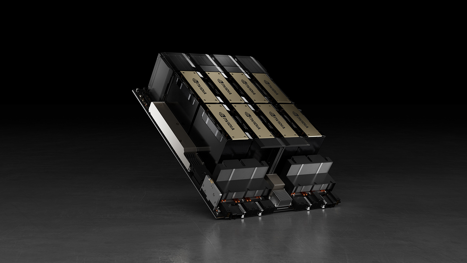
H20
96 GB HBM34.0 TB/sSXM5 / PCIe Gen5
H20
China compliance variant of the H100. Meets US export controls with reduced compute performance but retains full 96GB HBM3 memory and NVLink interconnect. Designed for large-model inference in the China market.
Quick Comparison
| GPU Model | VRAM | Bandwidth | FP16 | TDP | Starting Price |
|---|---|---|---|---|---|
| GH100 | 80 GB HBM3 | 3.35 TB/s | 1,979 TFLOPS (with sparsity) | 700W (SXM) / 350W (PCIe) | — |
| H100 SXM | 80 GB HBM3 | 3.35 TB/s | 1,979 TFLOPS (with sparsity) | 700W | — |
| H100 PCIe | 80 GB HBM3 | 3.35 TB/s | 1,513 TFLOPS (with sparsity) | 350W | — |
| H100 NVL | 94 GB HBM3 | 3.9 TB/s | 1,979 TFLOPS (with sparsity) | 350W | — |
| H200 SXM | 141 GB HBM3e | 4.8 TB/s | 1,979 TFLOPS (with sparsity) | 700W | — |
| H200 NVL | 141 GB HBM3e | 4.8 TB/s | 1,979 TFLOPS (with sparsity) | 350W | — |
| GH200 | 144 GB HBM3e (or 96 GB HBM3) | 4.8 TB/s (HBM3e) | 1,979 TFLOPS (with sparsity) | 1,000W | — |
| H800 SXM | 80 GB HBM3 | 3.35 TB/s | 1,000 TFLOPS (with sparsity) | 700W | — |
| H20 | 96 GB HBM3 | 4.0 TB/s | 148 TFLOPS (with sparsity) | 400W | — |
Why Choose Hopper?
Proven Performance
Hopper GPUs power the world's largest AI training clusters. Battle-tested in production at scale for LLM training, fine-tuning, and inference.
Cloud-Native Ready
Available across multiple cloud providers with hourly billing. Compare real-time pricing and pick the cheapest option for your workload.
Ecosystem Support
Full compatibility with PyTorch, TensorFlow, JAX, vLLM, TensorRT, and all major ML frameworks. NVLink for multi-GPU scaling.