AvailableHopper • 2022
H100 PCIe
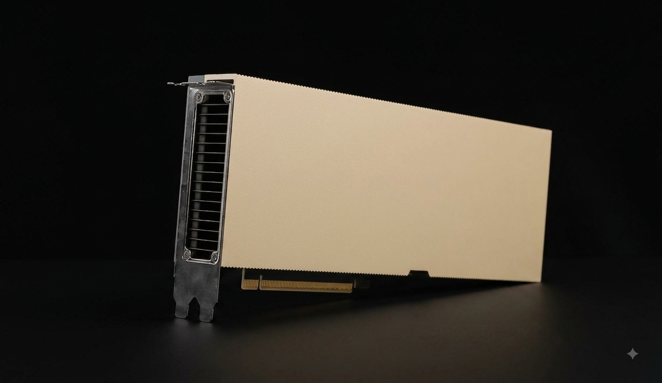
Standard PCIe Gen5 form factor of H100 (no NVLink). 350W TDP — lower performance than SXM but easier to deploy. No multi-GPU NVLink interconnect.
Technical Specifications
Architecture | Hopper |
Release Year | 2022 |
Process Node | TSMC 4N |
Form Factor | PCIe Gen5 |
VRAM | 80 GB HBM3 |
Memory Bandwidth | 3.35 TB/s |
Interconnect | PCIe Gen5 (128 GB/s) — no NVLink |
FP16 Performance | 1,513 TFLOPS (with sparsity) |
FP32 Performance | 51 TFLOPS |
FP64 Performance | 26 TFLOPS |
TDP | 350W |
CUDA Cores | 16,896 |
Tensor Cores | 528 |
Transistors | 80 billion |
Die Size | 814 mm² |
Best Use Cases
- AI inference
- Single-GPU training
- HPC
- Environments without SXM
Quick Facts
FamilyHopper
ArchitectureHopper
Released2022
ProcessTSMC 4N
Form FactorPCIe Gen5
Related Hopper GPUs
H100 PCIe — Frequently Asked Questions
What is the H100 PCIe GPU used for?
The H100 PCIe is best suited for: AI inference, Single-GPU training, HPC, Environments without SXM.
How much VRAM does the H100 PCIe have?
The H100 PCIe has 80 GB HBM3 of VRAM.
What is the memory bandwidth of the H100 PCIe?
The H100 PCIe has a memory bandwidth of 3.35 TB/s.
What interconnect does the H100 PCIe use?
The H100 PCIe uses PCIe Gen5 (128 GB/s) — no NVLink.
When was the H100 PCIe released?
The H100 PCIe was released in 2022.